Research
- +3
Nidhi Singh, Tejas Bharadwaj, Shruti Mittal, …
{
  "authors": [
    "Konark Bhandari"
  ],
  "type": "commentary",
  "centerAffiliationAll": "",
  "centers": [
    "Carnegie Endowment for International Peace",
    "Carnegie India"
  ],
  "englishNewsletterAll": "",
  "nonEnglishNewsletterAll": "",
  "primaryCenter": "Carnegie India",
  "programAffiliation": "",
  "projects": [
    "Technology and Society"
  ],
  "regions": [
    "India",
    "Europe"
  ],
  "topics": [
    "Technology"
  ]
}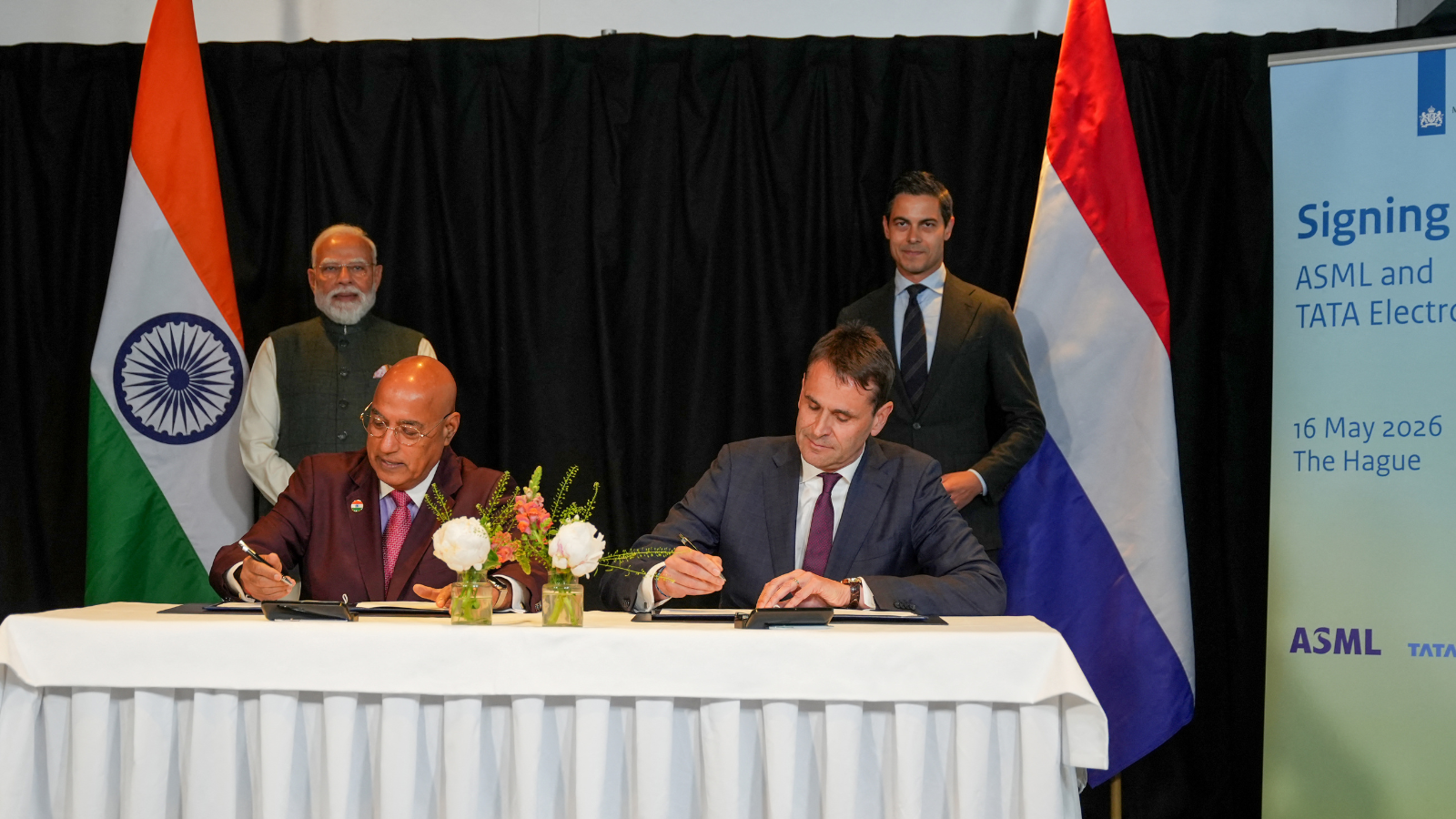
Source: Getty
The ASML MoU with Tata Electronics is an indicator of how far the Indian semiconductor ecosystem has come. This ecosystem has been years in the making and represents real commercial logic.
ASML, the Netherlands-based manufacturer of semiconductor lithography machines, recently signed a Memorandum of Understanding (MoU) with Tata Electronics—a partnership stated as critical to accelerating the setting up of the latter’s semiconductor fab in Dholera.
As first glance, this looks like a straightforward commitment to bolster semiconductor supply chains. Press releases from the two firms do little to suggest otherwise and Tata has recently signed MoUs with other key industry players as well, including Tokyo Electron, Merck Electronics, ROHM, and Intel. Individually, each MoU may not seem like much. But taken collectively, these developments point towards a deliberate effort to build a whole ecosystem in India. What this also indicates, is that since the announcement of the Dholera fab project in February 2024, the ecosystem has grown large enough to acquire the critical mass needed to attract major players like ASML.
This MoU comes on the back of a formal “Partnership on Semiconductors and Related Emerging Technology” between the governments of the Netherlands and India. Accordingly, a government-to-government push to work together on semiconductors is also likely. However, it is important to note that this semiconductor ecosystem has been years in the making and represents real commercial logic.
Since 2023, many semiconductor firms in the Netherlands, including ASML, have been largely restricted from selling semiconductor manufacturing equipment (SME) and tools to China, one of the largest markets in the world. Even its deep ultraviolet immersion (DUV) machines have come under the scanner, with some calling for even those to be restricted, since multi-patterning can produce more efficient AI chips and may help China close the gap on frontier AI in its competition with the United States. In a scenario like this, ASML has much to benefit by entering a new ecosystem in India which is still growing and nascent. Most SMEs have life cycles of several decades and it will arguably be harder to come in later, when decisions regarding procuring fab tooling equipment have already been made.
"Since the announcement of the Dholera fab project in February 2024, the ecosystem has grown large enough to acquire the critical mass needed to attract major players like ASML"
DUV machines, capable of manufacturing chips in the 28 to 90 nanometer range, are likely sufficient for India’s needs at this stage. The Tata fab in Dholera will produce 28 nanometer nodes, and could potentially process 14 nanometer nodes in the future. This is an easier sell for ASML compared to the more specialized extreme ultraviolet (EUV) machines, which India does not yet need, and are considerably more expensive.
However, India and the Netherlands would have to align on export controls norms for re-exporting such highly sensitive tech to other jurisdictions. India appears to already be laying the groundwork for this—the recent September 2025 revision to its export control laws, also called the SCOMET (Special Chemicals, Organisms, Materials, Equipment and Technologies) list, specifically singles out “advanced lithography tools with minimum resolvable feature sizes of 45 nanometres or less” as now being subject to stricter export control rules, even though, admittedly, India has “notified the items that are beyond the controlled list of the Wassenaar Agreement.”
ASML has previously stated a target of installing six hundred DUV machines globally by 2025–26. Given that China’s purchases of DUV machines may be restricted by the United States’ MATCH (Multilateral Alignment of Technology Controls on Hardware) Act, the question arises of how ASML plans to achieve this target. Could turning towards a growing Indian semiconductor ecosystem be part of the answer? Interestingly, despite the possibility of restricted export controls, if the MATCH Act is passed, as of April 2026, ASML still raised its sales forecast for 2026.
It is worth asking whether the India Semiconductor Mission (ISM) 2.0 could incentivize the deployment of refurbished equipment in India as well. According to its 2025 annual report, ASML actively monitors systems that remain in use, “including our EUV, DUV and PAS 5500 systems,” and both ASML and its customers have a shared interest in extending the lifespan of these machines, given their high value. In 2025, ASML sold twenty-seven refurbished lithography systems; to date, they have refurbished and resold over 600 such systems; and by the end of 2025, of all the refurbished systems they sold in the past thirty years, 95 percent were still active. Accordingly, refurbished equipment could represent a huge play for ASML in India as a cost-effective option.
It is also important to clarify that EUV machines are not essential to making better chips. Over the past decade, firms that adopted EUV machines too early have faced problems with yield.1 Meanwhile, firms like Micron that pursued the singular adoption of DUV machines, optimized them and eventually made dynamic random-access memory (DRAM) chips more efficiently, achieving greater node density.2 Therefore, India’s increasing appetite for DUV machines is not necessarily a bad thing at all. In fact, the demand for mask sets (stencils that etch patterns on silicon wafers) for trailing edge chips has also seen a surge. As per ASML and eBeam Initiative, the demand for mask sets for nodes larger than 28 nanometers has increased by 40 to 48 percent. The Dholera fab will manufacture trailing edge nodes, and this makes India a natural market for ASML to target as it looks to place more DUV machines globally.
In the end, the ASML MoU with Tata Electronics is an indicator of how far the Indian semiconductor ecosystem has come. The ecosystem in Dholera in particular, has matured and now reached the critical mass where major semiconductor firms can enter with the confidence that this ecosystem will only grow, with the Dholera fab being “strongly positioned to realize its ambitions.” The challenge will be to sustain the overall momentum and towards this, the upcoming ISM 2.0 scheme may well play a pivotal role.
Fellow, Technology and Society Program
Konark Bhandari is a fellow with Carnegie India.
Recent Work

Nidhi Singh, Tejas Bharadwaj, Shruti Mittal, …
Konark Bhandari
Carnegie India does not take institutional positions on public policy issues; the views represented herein are those of the author(s) and do not necessarily reflect the views of Carnegie, its staff, or its trustees.
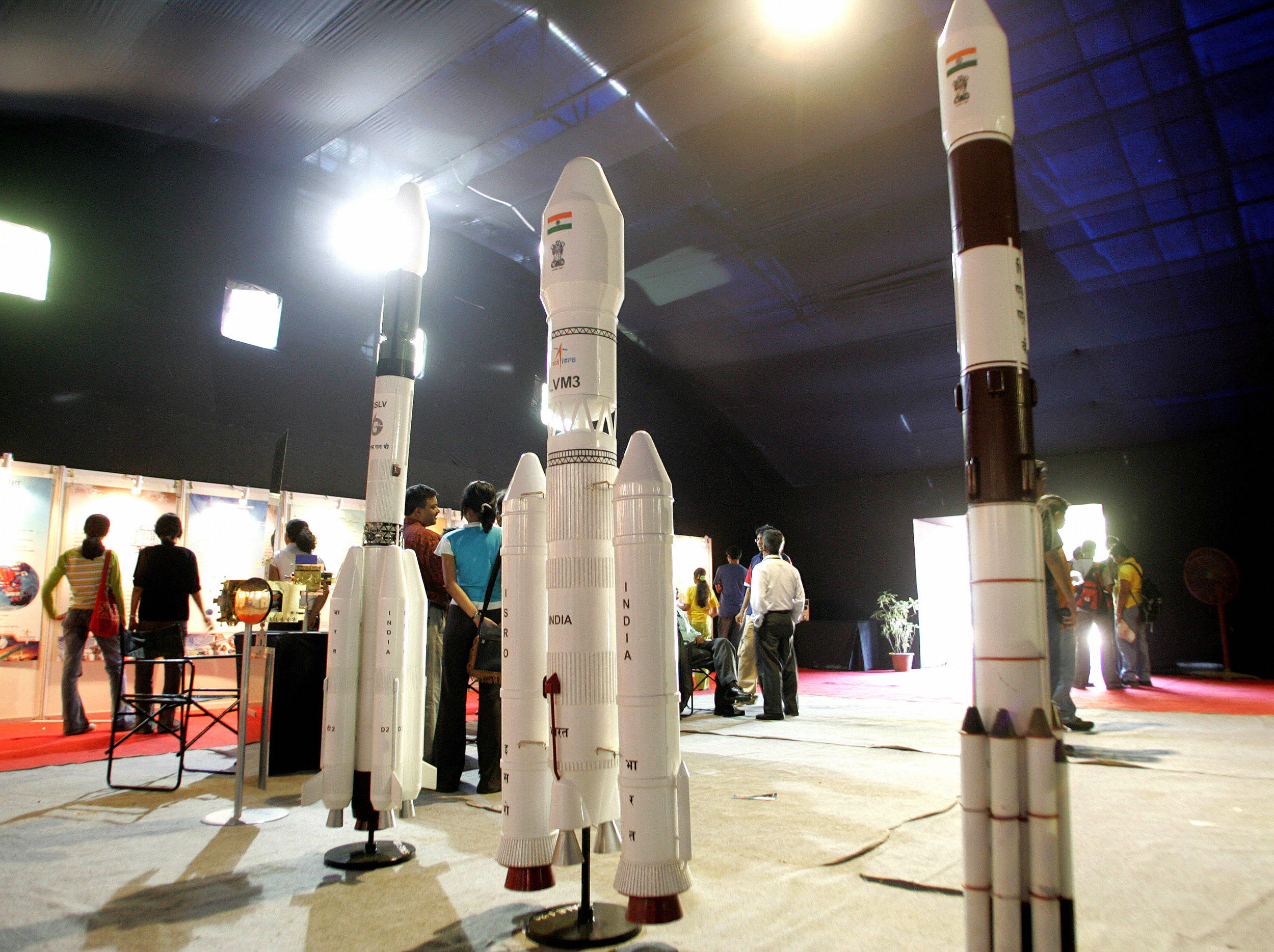
This paper examines the relationship between India’s evolving space policy and the corresponding growth in private space ventures. It analyzes both the enabling factors created by recent regulatory changes and the persistent challenges facing entrepreneurs in this capital-intensive, highly regulated industry.
Harshan Vazhakunnam
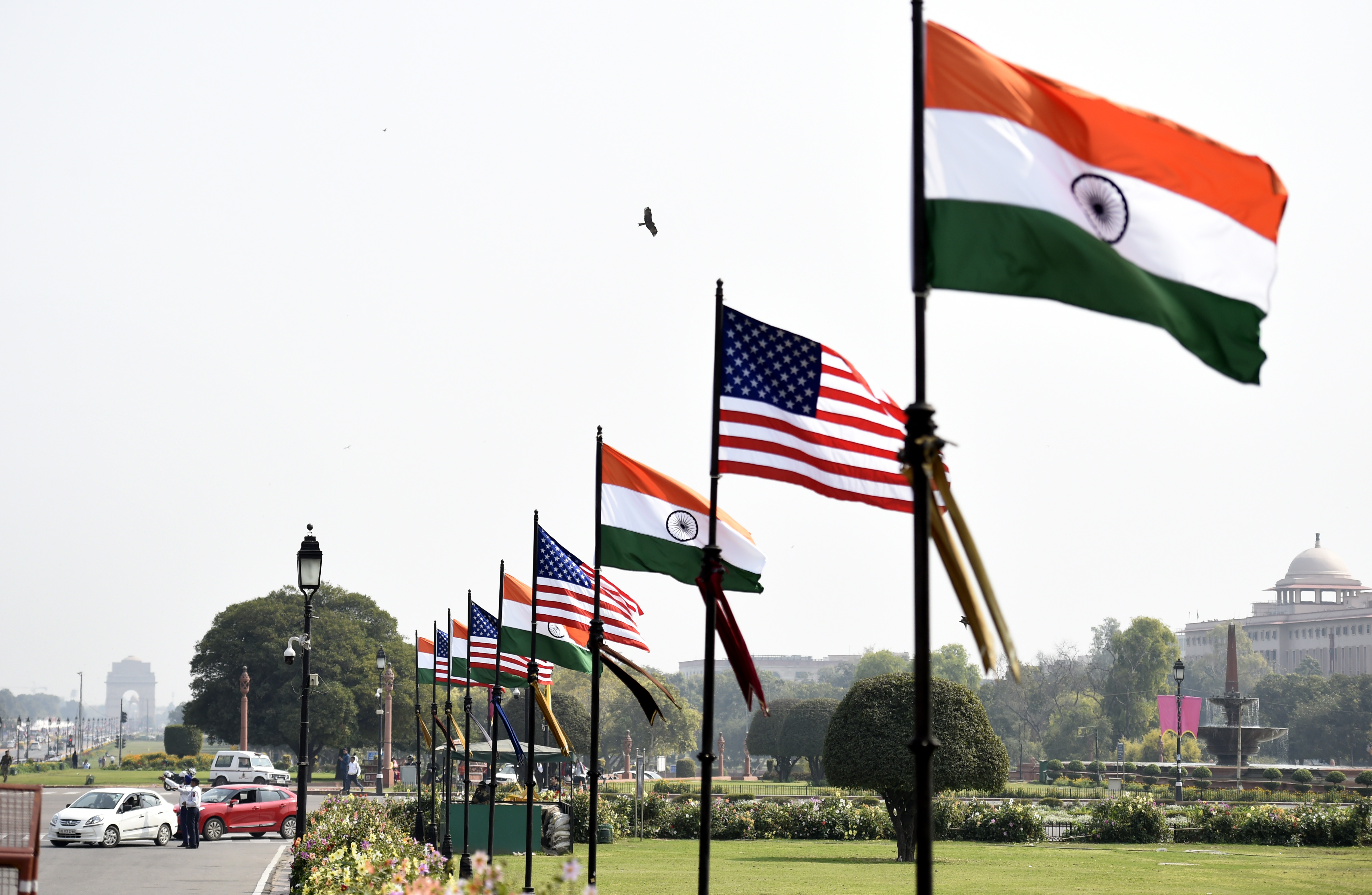
The U.S.–India semiconductor cooperation story is well-stocked with top-level strategic intent. What remains unresolved, however, are some underlying challenges that will determine whether the cooperation actually functions. Three such friction points stand out.
Shruti Mittal

Drawing on ten public discussions from the India AI Impact Summit 2026, this article highlights key outlooks on open source in AI that are likely to shape policy and governance conversations going forward.
Shruti Mittal
This collection of essays by scholars from Carnegie India’s Technology and Society program traces the evolution of the AI summit series and examines India’s framing around the three sutras of people, planet, and progress. Scholars have catalogued and assessed the concrete deliverables that emerged and assessed what the precedent of a Global South country hosting means for the future of the multilateral conversation.
Nidhi Singh, Tejas Bharadwaj, Shruti Mittal, …
On March 10, 2026, India’s Union Cabinet approved amendments to Press Note 3, a regulation that mandated government approval on all foreign direct investment (FDI) from countries sharing a land border with India. This amendment raises questions primarily about whether its stated benefits will materialize and if the risks have been adequately weighed. This piece will address the same.
Konark Bhandari